 Corexis Memory
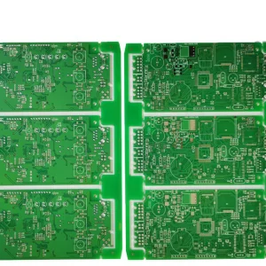
Engineered high-thermal MCPCBs and OEM modules to deploy 260nm-270nm 3535 UVC LED packages efficiently in commercial sanitization systems.

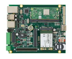
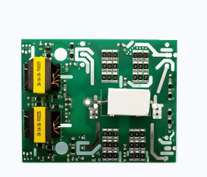
An authoritative analysis of optical physics, thermal management, and European deployment regulations for automated deep-UV sanitization.
The microbial inactivation efficiency of ultraviolet radiation relies heavily on the optical absorption characteristics of cellular nucleic acids (DNA and RNA). The peak germicidal absorption cross-section resides between 260nm and 265nm. Within this narrow spectral range, UVC photons induce the formation of cyclobutane pyrimidine dimers (CPDs) in DNA strands. These covalent bonds prevent transcription and replication, rendering pathogens inert.
While traditional low-pressure mercury lamps emit a static line at 253.7nm, advanced solid-state 260nm-270nm 3535 UVC LEDs offer targeted emission matching the DNA absorption curve. This ensures up to a 30% higher disinfection efficacy per milliwatt of optical output. When integrated on high-thermal-conductivity metal-core printed circuit boards (MCPCBs), these light sources achieve robust sanitization without chemical byproducts.
Solid-state UVC emitters feature a low External Quantum Efficiency (EQE), generally converting 2% to 6% of electrical energy into optical radiation. The remaining 94%+ is converted into heat. Since UVC LED junction temperatures directly affect optical power degradation and lifetime, thermal management is a critical parameter.
The 3535 ceramic package (3.5mm x 3.5mm footprint) provides a compact, surface-mount layout. However, it requires a dedicated thermal path to dissipate heat. Our custom Aluminum PCB T6 3535 lamp bead substrates utilize a high-performance dielectric layer to deliver a low thermal resistance path. This preserves the internal junction temperature below 60°C, maintaining the device's operational lifespan (>15,000 hours L70) and preventing premature wavelength shift.
| Parameters | Specifications (Typical) | Design Impact on Disinfection |
|---|---|---|
| Peak Wavelength Range | 260nm - 270nm | Maximum overlap with germicidal DNA absorption peak |
| Package Dimensions | 3.5mm x 3.5mm (3535 ceramic) | High power density, easy SMT integration on circular arrays |
| Forward Voltage (Vf) | 5.0V - 7.5V per chip | Determines driver board and constant-current power design |
| Thermal Conductivity (Substrate) | 1.5 - 3.0 W/m·K (Al T6 Substrate) | Prevents thermal runaway and maintains constant radiant flux |
| Beam Angle Options | 60° (focused) / 120° (flat window) | Optimized for static surface scan or fluid flow reactors |
As the European Union intensifies its environmental directives, Portugal's industrial sectors are shifting toward clean, chemical-free disinfection. In regions like Lisbon, Porto, and Algarve, municipal water treatment facilities are replacing chlorine-dosing systems with UV arrays to eliminate disinfection byproducts (DBPs). Our SMT PCBA capabilities and 3535 Aluminum substrates are designed to support local Portuguese clean-tech manufacturers in assembling CE and RoHS-compliant UVC modules.
Furthermore, Portugal's expanding aquaculture, food processing, and wine sectors are deploying localized automated air and conveyor surface sterilization. By incorporating 260nm-270nm UVC LED systems into these process lines, local businesses can extend product shelf lives, improve hygiene standards, and meet EU food safety compliance without chemical additives.
Leveraging advanced SMT infrastructure, reliable components, and high-standard quality assurance to support global supply chains.
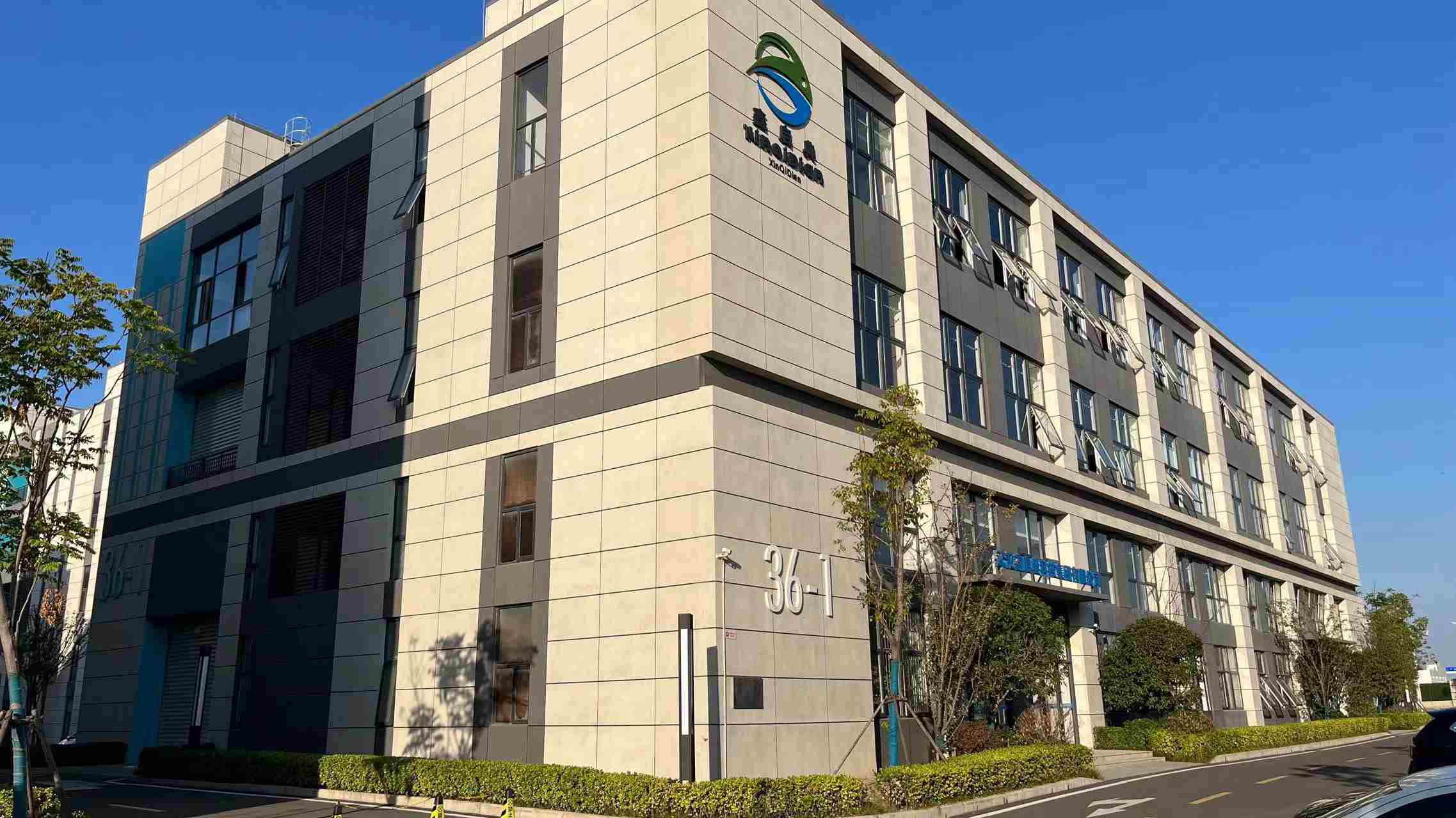
Founded in 2016, Corexis Memory Technology Co., Ltd. operates a modern manufacturing facility covering 21,800 m². While we are a leading designer of high-speed DDR4/DDR5 DRAM and industrial memory modules, our manufacturing infrastructure is built on advanced surface mount technology (SMT) lines and lead-free HASL PCB processing. This versatility allows us to deliver high-quality, high-thermal aluminum substrates and controller boards for industrial applications worldwide.
Our engineering team of 128 R&D professionals provides comprehensive customization services, including hardware development, firmware optimization, and custom PCB layout designs. This technical expertise ensures that our products meet the strict standards required by municipal and industrial systems in Portugal and across Europe.
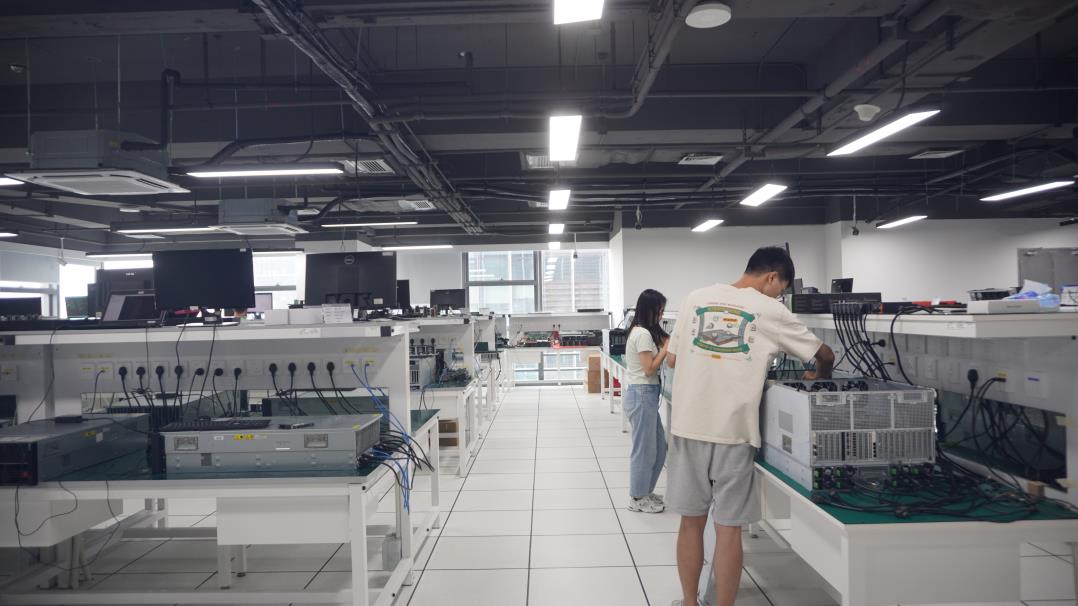
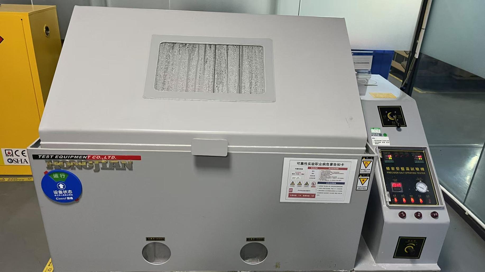
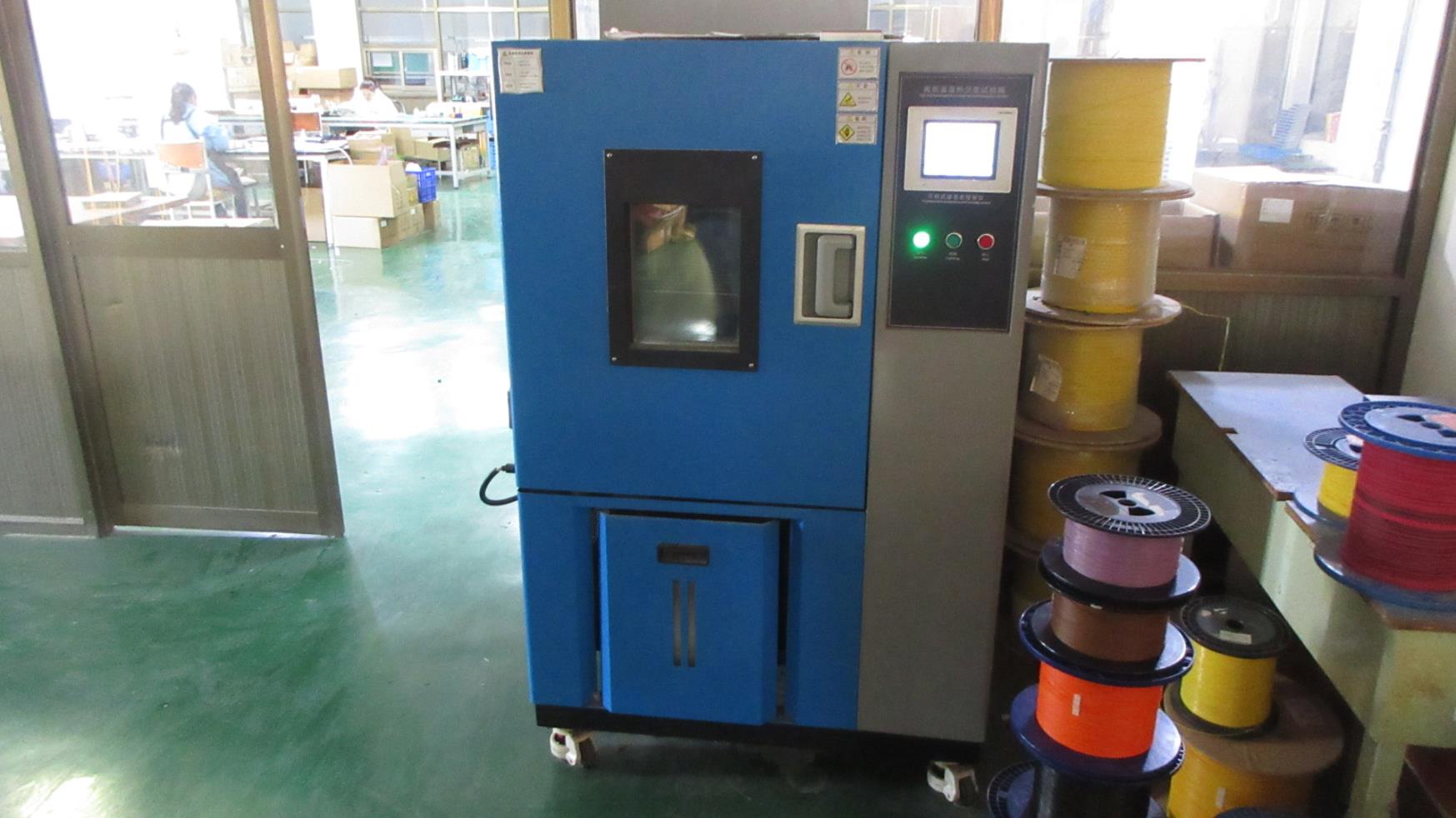

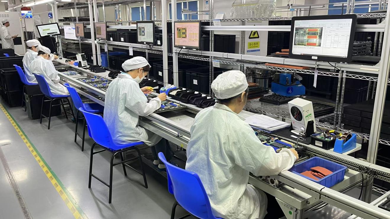
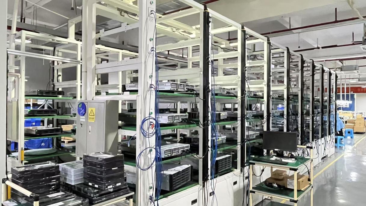
High-reliability DRAM solutions for European municipal data collection, smart IoT gate systems, and automated SCADA networks.
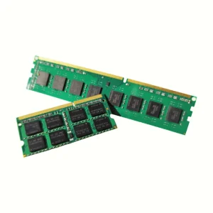
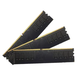
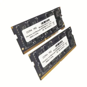
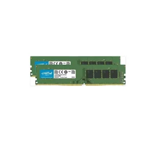
Explore our certified product line, featuring 100% full inspection and strict compatibility matching for European system integration.
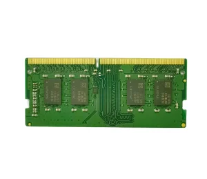
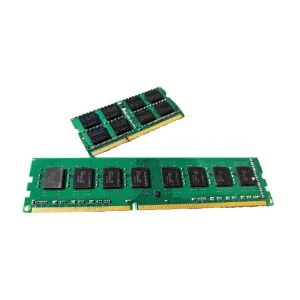
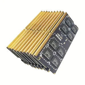
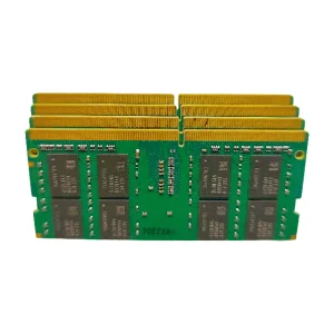
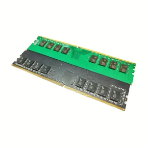
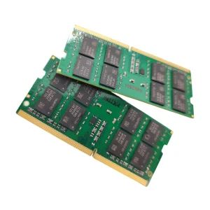
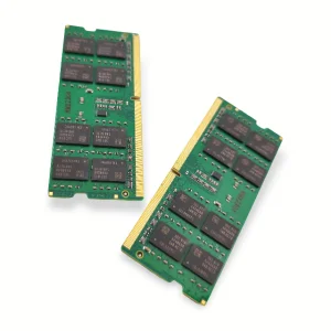
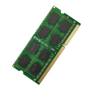
How Corexis ensures strict quality control and technical compliance for high-demand international markets.
In global electronic manufacturing, product reliability is key. Corexis operates under a strict Quality Management System, employing 56 dedicated quality control personnel to manage every stage of production. From incoming raw materials to final shipping inspections, our quality controls ensure compliance with European standards like CE, RoHS, and WEEE.
Whether you require customized copper-core PCBs for 3535 UVC arrays or specialized controller designs, Corexis offers flexible customization options. Our SMT packaging and OEM services include customized PCB layouts, capacity configuration adjustments, thermal simulation profiling, and private label packaging to fit your brand's specifications.
Technical advice and answers regarding wavelength selection, thermal design, and OEM integration for 3535 UVC LEDs.
The peak absorption of DNA and RNA in bacteria and viruses occurs between 260nm and 265nm. Within this range, UVC energy disrupts the molecular bonds of pathogens, preventing them from reproducing. Compared to 275nm or 280nm options, the 260nm-270nm spectrum delivers higher germicidal efficiency per milliwatt.
UVC LEDs convert over 90% of their electrical input into heat. If this heat is not dissipated, the junction temperature rises, causing rapid optical degradation and a reduction in lifespan. An Aluminum PCB (MCPCB) with high thermal conductivity (e.g., T6 substrate) provides an efficient thermal pathway to keep the LED package cool.
Yes. Through our SMT PCBA divisions, we offer custom hardware development, firmware optimization, and SMT assembly. We can integrate driver modules, timer controllers, and industrial communication protocols for automated sanitation networks.
Yes, all products manufactured at our facility comply with RoHS and CE standards. We use lead-free HASL or OSP surface finishes and resin plug vias to ensure the durability and environmental safety of our electronic assemblies.
Standard prototype runs for 2-layer HASL or aluminum-core PCBs are completed within 5-7 working days. Bulk production lead times vary from 12 to 18 days, depending on component availability and the specific testing requirements.
We perform a 100% full inspection process. This includes Incoming Quality Control (IQC) for components, In-Process Quality Control (IPQC) during assembly, and Final Quality Control (FQC) alongside Outgoing Quality Assurance (OQA) testing prior to shipment.
Contact Corexis's application engineers to request samples, schedule thermal testing simulations, or obtain quotes for bulk PCB/PCBA manufacturing.