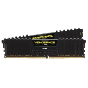
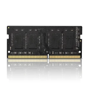
A premier global OEM/ODM manufacturer specializing in high-frequency multilayer substrates, industrial PCBs, and enterprise-grade DRAM memory solutions.
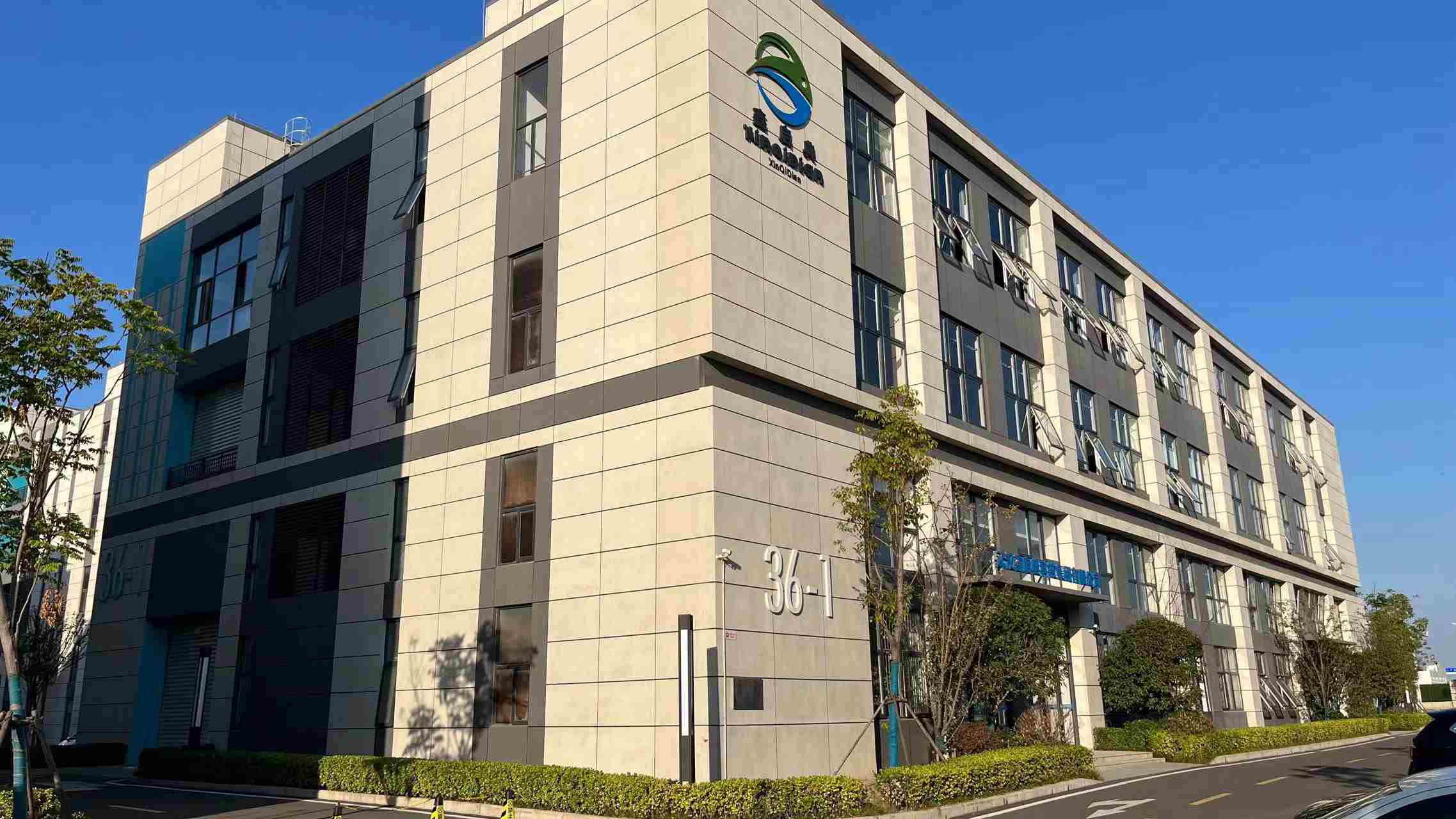
Founded in 2016, Corexis has stood at the cutting edge of memory architecture and advanced electronic manufacturing services (EMS). Operating from our modern 21,800 m² manufacturing facility, we integrate complete hardware design, multi-layer high-frequency PCB prototyping, SMT patching, and rigorous validation tests under one roof. Originally established to fulfill high-speed DRAM memory solutions, we have expanded our capacity to engineer complex multilayer systems for global system integrators and industrial partners.
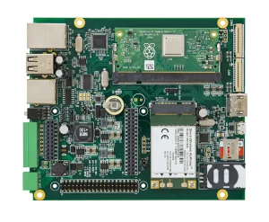
Our deep vertical integration guarantees that we control quality down to the trace impedance levels of our multi-layer boards. Whether engineering custom server boards or designing memory substrates with high TG170 material, our engineering core delivers precision, stability, and scale.
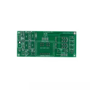
From edge computing hardware to high-power industrial machinery, multi-layer circuit boards form the neural network of modern technology.
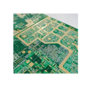
Supporting rapid data flow requires signal pathways that minimize latency and insertion loss. Our multi-layer boards utilize low-loss materials such as Rogers 4000 series mixed with high TG170 FR4 to deliver exceptional electromagnetic integrity for telecom base stations, high-bandwidth routers, and IoT gateways.
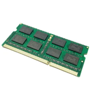
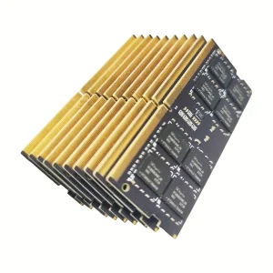
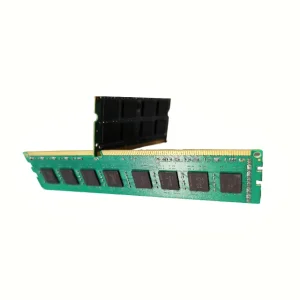
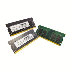
Modern servers demand extreme DRAM capacity and speeds. Fabricating high-density memory substrates like DDR4 and DDR5 modules requires sub-micron tolerances, blind/buried microvias, and specialized gold finishes. We build circuits that withstand the continuous thermal cycles of hyperscale datacenters.
In high-power environments, such as welding inverter systems and mining detectors, electrical noise and extreme temperature variations can disrupt circuit operations. Corexis multilayer boards are engineered with thick copper layers (up to 3oz) and high glass-transition (Tg) points to survive these industrial demands.
Technical capabilities built to handle high routing densities and rapid switching cycles with minimal signal distortion.
Creating high-frequency platforms like our Rogers 4000 Mixed Pressure modules or high-layer count FR4 designs requires rigorous physical parameters. Our machinery handles line width/spacing limits down to 3mil (75μm), utilizing automated optical inspection (AOI) to eliminate structural errors before chemical etching. By employing sequential lamination and precise laser drilling, our engineers create high-aspect-ratio vias designed to guarantee conductivity under extreme thermal loads.
| Parameters | Standard Capabilities | Advanced Capabilities |
|---|---|---|
| Layer Count | 2 to 16 Layers | Up to 32 Layers | Base Materials | FR4 (Shengyi, Kingboard) | Rogers 4003C/4350B, High-TG (TG170/TG180) |
| Board Thickness | 0.4mm to 2.4mm | 0.2mm to 3.2mm |
| Copper Thickness | 0.5 oz to 2.0 oz | Up to 6.0 oz (Heavy Copper) |
| Min. Line Width/Spacing | 4 mil (0.1mm) | 3 mil (0.075mm) |
| Impedance Tolerance | ±10% | ±5% |
| Surface Finishes | HASL, Lead-Free HASL, OSP | ENIG (Immersion Gold), Hard Gold Plating, ENEPIG |
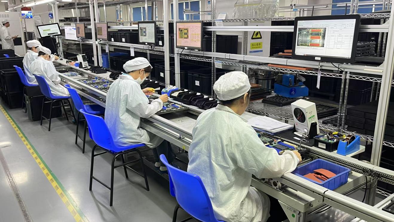
Our manufacturing complex integrates multi-stage surface mount technology (SMT) with visual check lines. This ensures components like RAM chips, controllers, resistors, and connectors are mounted with absolute precision. By linking substrate design directly to our high-precision mounting processes, we eliminate trace compatibility issues, boosting yield rates and device lifespans.
How Corexis handles regional engineering standards, material sourcing regulations, and custom design pipelines.
We build all circuit systems to satisfy the most demanding regulatory frameworks. Corexis multi-layer boards are fabricated under ISO 9001:2015 and ISO 14001:2015 standards, ensuring full UL-certified material tracking and RoHS/REACH environmental compliance for standard entry into EU and US markets.
Our R&D team works with system integrators to customize PCB sizes, layer stacks, thermal vias, and surface plating. With flexible volume options, we accommodate rapid prototype runs for early-stage validation as well as massive production runs exceeding millions of pieces.
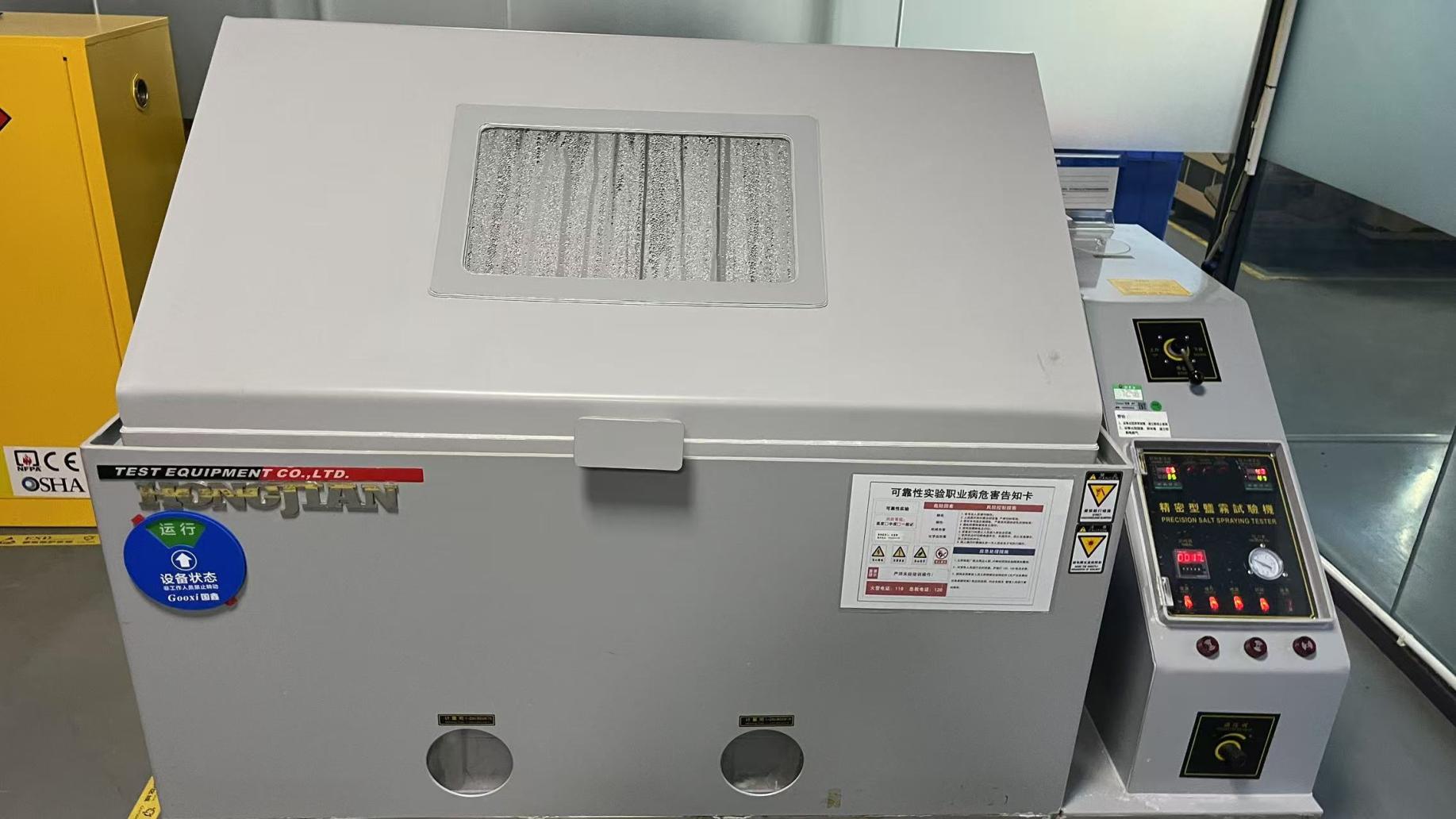
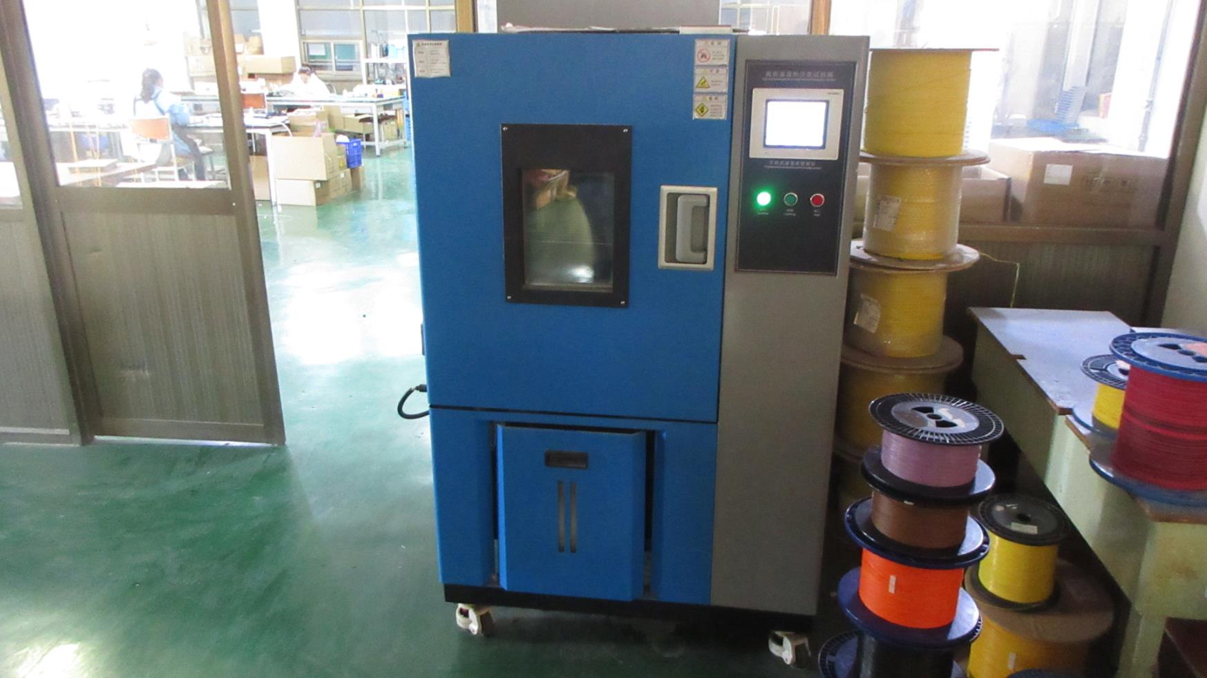
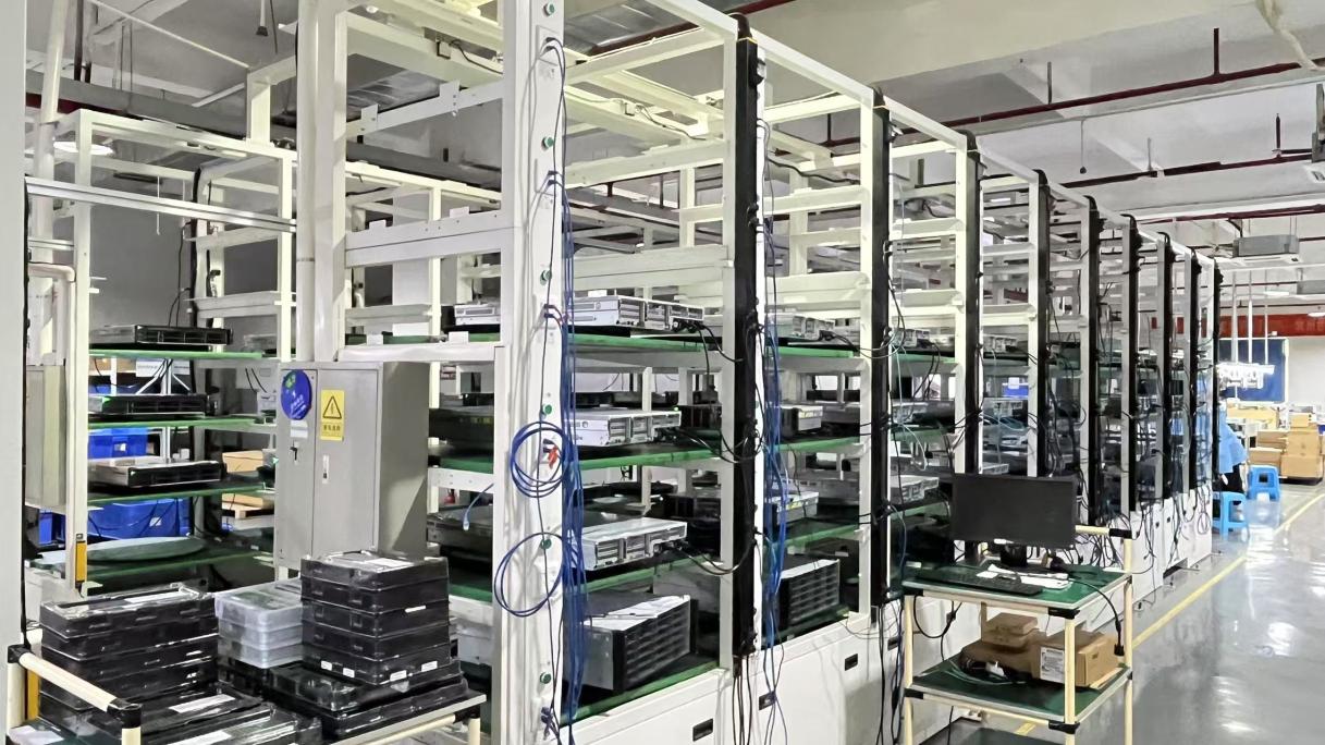
Every single board undergoes extensive testing. Our process utilizes Incoming Material Inspection (IQC), In-Process Quality Control (IPQC), Final Quality Control (FQC), and Outgoing Quality Assurance (OQA). We also execute rigorous reliability tests, including thermal shock, solderability, and compatibility sweeps.
Driving advancements in substrate structures, material engineering, and ultra-high-speed signaling architectures.
As microprocessors reduce their pin pitches, standard layout methods reach physical limits. Corexis is advancing its Any-Layer HDI technology, utilizing laser microvias and ultra-thin substrates to accommodate dense signal matrices on boards with up to 32 layers.
With data transfer speeds climbing past 6400MT/s, we are engineering substrates featuring ultra-low-loss dielectric properties. These designs incorporate specific trace shielding to limit crosstalk and reflection on high-frequency channels.
To support global sustainability goals, Corexis is reducing environmental impacts across our supply chain. We are developing manufacturing techniques that use halogen-free base materials, lead-free surface finishes, and recycling processes to reuse excess copper and water during production.
Answers to crucial engineering questions regarding multilayer circuit board specifications, material attributes, and manufacturing processes.
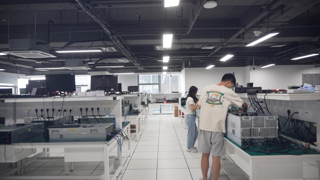
Inside Corexis: A cleanroom SMT production floor featuring automated component placement and validation equipment.

 Corexis Memory